Over the course of human history, climates have changed, civilizations have risen and fallen, languages have evolved, and political boundaries have been redrawn. Yet one thing has remained remarkably constant: the desire to develop better technologies and improve the way we live. In the 21st century, when semiconductors are the cornerstone of every technology, this desire is met by improvements in transistor technology. For several decades, the semiconductor industry improved transistor performance using a remarkably successful strategy: making the transistors smaller. By shrinking the dimensions of conventional planar transistors, or MOSFETs, engineers were able to increase speed, reduce power consumption, and pack more transistors onto a chip. This trend, often associated with Moore’s Law, drove the rapid advancement of computers, smartphones, and countless other electronic devices.
However, by the early 2000s, engineers began to encounter fundamental physical limitations. The transistors had become so small that it was no longer possible to continue shrinking their dimensions. To overcome these challenges, the industry introduced a fundamentally different transistor architecture: the FinFET. Commercialized at leading-edge technology nodes around 2011, FinFETs extended transistor scaling by improving electrostatic control of the channel. A decade later, the industry began transitioning again, this time toward Gate-All-Around (GAA) transistors, which provide even stronger gate control.
Why did conventional planar scaling eventually reach its limits? Why did engineers abandon a strategy that had worked so well for decades? In this article, I’ll explain the transition from planar MOSFETs to FinFETs—and ultimately to GAA transistors—using a simple analogy.
Please keep in mind that the words MOSFET and transistor are used interchangeably, and mean the same thing for the purpose of this blog.
A Simple Analogy for Understanding a Transistor
Modern digital electronics are built using a device called the metal-oxide-semiconductor field-effect transistor, or MOSFET. The MOSFET has three primary terminals: the source, drain, and gate (Figure 1). Its job is simple: use the gate to control the flow of current between the source and drain through a region called the channel.
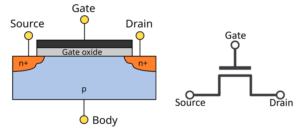
Figure 1. FET cross-section (left) and circuit schematic (right). Left figure adapted from [1]
To develop an intuitive understanding of how a transistor works, let’s build an analogy.
Imagine a long, narrow room formed by joining two buildings side by side with a gap between them (Figure 2). Alice stands at one end of the room, and Bob stands at the other. Alice represents the source, Bob represents the drain, and the air medium between them represents the channel through which information—or, in the case of a transistor, electrical current—can travel.
A third person, Gary, controls whether Alice and Bob can communicate. Gary represents the gate. He sits above the room and has access to a large wooden block that can be lowered into the gap between the buildings. When the block is lowered, communication between Alice and Bob is blocked. This corresponds to the transistor’s OFF state, where the gate prevents current from flowing between the source and drain. When the block is lifted, Alice and Bob can talk freely. This corresponds to the transistor’s ON state, where current is allowed to flow through the channel.
Like all analogies, this one is not a perfect representation of the underlying physics. However, it captures the central idea of transistor operation: the gate controls communication between the source and drain.
| OFF state | ON state | |
| FET | Gate=off, no current flow | Gate=on, current flows between source and drain |
| Block analogy | Block inserted, Alice and Bob can’t talk | Block lifted, Alice and Bob can talk |
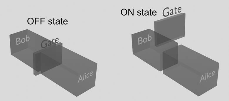
Figure 2. Block analogy demonstrating FET operation. (left) OFF state, (right) ON state.
Why Shrinking Transistors Stopped Working
Now that we have established the analogy, let’s talk about transistor scaling.
Scaling is the process of reducing the physical dimensions of a transistor. For decades, this was the primary engine driving improvement in semiconductor technology. Engineers reduced the channel length, thinned the gate oxide, and optimized other device dimensions to create smaller and faster transistors. The results were remarkable. Smaller transistors could switch faster, consume less power, and occupy less chip area. This allowed manufacturers to place more transistors on a chip while simultaneously improving performance and energy efficiency. For consumers, the benefits were obvious: computers became faster, smartphones became more capable, and battery life improved from one generation to the next.
However, this strategy eventually encountered a fundamental problem. As the channel length became extremely small, the gate’s ability to control the channel began to weaken. Current could no longer be completely shut off when the transistor was supposed to be in its OFF state. This phenomenon is broadly associated with short-channel effects, which become increasingly severe as device dimensions shrink.
Returning to our analogy, shrinking the channel length is equivalent to shortening the room and bringing Alice and Bob closer together. When Alice and Bob are far apart, the wooden block effectively prevents communication. Tiny imperfections around the edges of the block do not matter because their voices are too weak to travel through the small openings.
As Alice and Bob move closer together, however, those same openings become significant. Even with the block in place, some sound can leak around the edges, allowing limited communication.
Similarly, in a scaled transistor, current begins to leak between the source and drain even when the gate is trying to turn the device off. This leakage current wastes power and increases heat generation. For battery-powered devices, it reduces standby time. More importantly, it signals that the conventional strategy of simply making planar transistors smaller is approaching its limits.
The semiconductor industry needed a new solution.
The move from planar MOSFETs to 3D FinFETs
This is where FinFETs enter the story.
Engineers realized that the root of the problem was insufficient electrostatic control of the channel. If the gate could exert stronger control over the channel, transistor scaling could continue. The solution was surprisingly elegant: instead of placing the gate only on top of the channel, wrap the gate around multiple sides of it. This idea is similar to wrapping yourself in a blanket on a cold day—the more completely you are surrounded, the greater the effect.
To make this possible, engineers modified the transistor geometry. Rather than forming the channel entirely within the plane of the chip, they raised it into a narrow vertical “fin” that protrudes from the surface. The gate could then cover the top and both sidewalls of this fin, allowing it to influence the channel from three directions simultaneously (Figure 3). The additional gate coverage dramatically improves electrostatic control and suppresses leakage current.
Because the gate surrounds three sides of the channel, Intel referred to its implementation as a tri-gate transistor. The industry more commonly uses the term FinFET.
Wrapping the gate around three sides of the channel can be viewed, in our analogy, as adding two additional wooden blocks from the sides of the room (Figure 4). These extra barriers close many of the pathways through which Alice and Bob could communicate when they were brought closer together. As a result, Alice and Bob can move closer than before while Gary still maintains effective control over their communication. In transistor terms, the channel length can be reduced further without suffering unacceptable leakage current.
This innovation gave the semiconductor industry another decade of transistor scaling and enabled continued improvements in computing performance, energy efficiency, and transistor density.
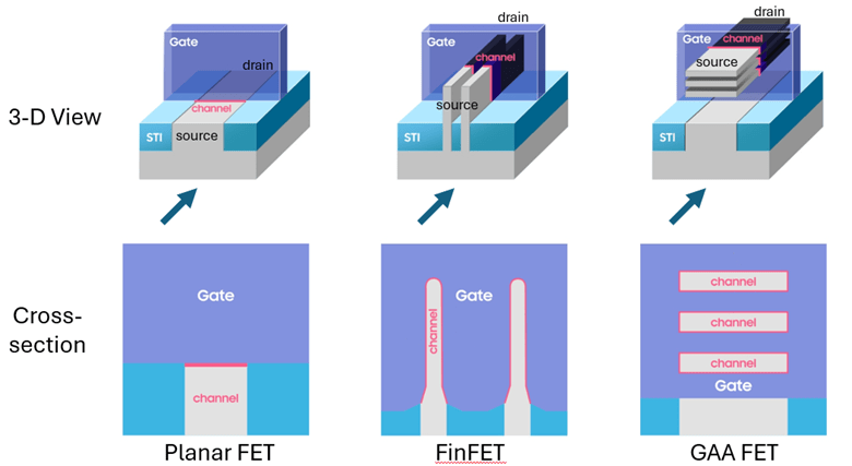
Figure 3. 3-D view and cross-sectional view, as seen from the direction of the arrow, of planar FET, FinFET, and GAA FET. Figure reproduced from [2].
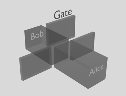
Figure 4. Representation of FinFET in the block analogy.
From FinFETs to Gate-All-Around Transistors
Eventually, however, even three-sided gate control reached its limits.
If Alice and Bob continue moving closer together, they will eventually discover new paths through which sound can leak. To regain control, Gary needs one final improvement: a fourth barrier placed underneath the room.
The transistor equivalent is to surround the channel completely with the gate. This architecture is known as a Gate-All-Around (GAA) transistor because the gate wraps around all sides of the channel.
By providing even stronger electrostatic control than a FinFET, GAA technology allows transistor scaling to continue beyond the practical limits of FinFETs.
A little exercise for your brain
GAA leads to an interesting fabrication challenge.
Creating a FinFET is relatively straightforward because the channel remains attached to the silicon substrate. The substrate provides mechanical support while exposing the top and side surfaces of the channel to the gate.
A GAA transistor is different. The gate must surround the entire channel, including its underside. If one were to simply remove the substrate beneath a FinFET channel, the structure would lose its support and collapse.
So how do semiconductor engineers fabricate a channel that is effectively suspended while still maintaining mechanical integrity throughout the manufacturing process? To fabricate GAA, you need a magical power to keep the channel floating in the air until you can wrap it with a gate and provide some mechanical support. Just kidding. The answer involves a series of ingenious fabrication techniques that allow the channel to remain supported until the gate structure is formed. Exploring those techniques is a fascinating topic in its own right and deserves a separate discussion.
The Story Continues
The story of transistor scaling doesn’t end with GAA transistors. Just as planar transistors eventually gave way to FinFETs, and FinFETs are now giving way to GAA devices, it is only a matter of time before GAA technology reaches its own limits. Engineers are well aware of this challenge and have already begun exploring future transistor architectures such as complementary FETs (CFETs) and transistors based on transition metal dichalcogenides (TMDs). Are you excited about these emerging technologies? I certainly am.
References
[1] https://en.wikipedia.org/wiki/Field-effect_transistor
Acknowledgement
During the writing process, I utilized AI assistance from ChatGPT to refine my ideas and improve the structure of this post.

Leave a comment